


VOLCANO® semi IGBT Laser Optics
Systems > Semiconductor Processing
Laser Optics for green IGBT Laser Backside Annealing & Ohmic Contact Formation on SiC.
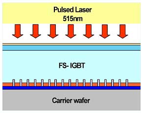
Laser activation of bonded IGBT.
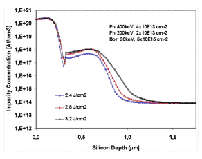
Activated Boron and Phosphorous dopant measured by SRP (courtesy FhI ISIT, Itzehoe).
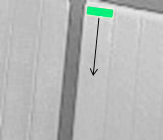
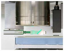
The color of the Ni coated SiC is changing from grey to silver after laser treatment (green laser line length ~3mm).
The depth of the activation process is precisely controlled by selecting the laser beam parameters pulse duration, line width and scan speed. The Phosphorous fieldstop layer of an IGBT can be activated up to 2 µm deep. The VOLCANO® Laser Optics is either operated with a single or with two homogenizer coupled laser sources, depending on throughput requirements.
SiC high power electronics require ohmic contacts with low electrical resistance to avoid power losses and heating. The ohmic contacts are made from evaporated magnetron sputtered Ni of typical 200nm thickness. The electrical resistance into the semiconductor device is reduced 20% by using a green laser exposure.
Scope of Application
IGBT´s (insulated gate bipolar transistors) are processed on thinned wafers with a thickness of 100µm or less. Often these thinned wafers are mechanically stabilized by using the so-called TAIKO grinding process (DISCO Corp., Japan) and a protection tape on the already processed front side. This tape is not compatible with high process temperatures. If the activation is performed with the VOLCANO® semi IGBT Laser Optics, an activation rate of >75% can be achieved for both, the fieldstop and the emitter layer. The tape stays intact during this high temperature process.
SiC MOSFET inverter and SiC high power diodes require ohmic contacts with low electrical resistance to avoid power losses and heating. TiN, SiNi, Ni2Si and Ni are ohmic contact materials to n-type SiC. The ohmic contacts are made from evaporated magnetron sputtered layers of typical 200nm thickness. The electrical resistance into the semiconductor device is minimized by using a laser exposure to generate void-free Ni2Si. A pulsed 532nm laser line providing 4-6 J/cm2 energy density is scanned over the Ni-coated SiC wafer at a typical scan speed of 60mm/s. The pulsed energy deposition creates the NiSi, Ni2Si compound without heating the SiC bulk material and the semiconductor device can be completed without any risk of damage.
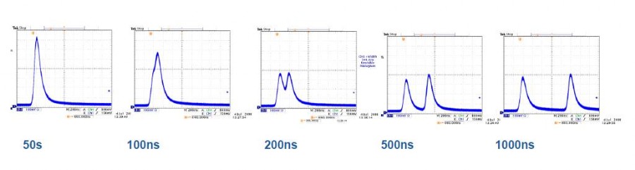
The combination of two laser pulses with controlled delay gives optimization of dopant activation and ohmic cntact formation.
Features
VOLCANO® semi IGBT Laser Optics:
g200 or Revolution 40/80 combined with FALCON® line beam optics.
g200 or Revolution 40/80 combined with FALCON® line beam optics.
| Technical Data | ||
Line length: | 2 - 5 mm (FWHM) | |
Homogeneity: | 6 sigma <=5 % | |
Wavelength | 527, 532 nm | |
| Line width: | 30 µm FWHM typical | |
Energy density: | max. 5,000 mJ/cm² | |
| Pulse duration: | variable 300, 500ns, double pulse synchronization | |
Laser: | g200, Revolution 40/50 (Spezifications by laser manufacturer on request) | |
| Beam profile measurement: | CCD Camera with microscope objective | |
VOLCANO® Laser Optics includes an integrated attenuator module to adjust the energy density at the substrate level. Power meter heads and a CCD camera based beam profile measurement are available. VOLCANO® Laser Optics has high availability (>90 %), is reliable and has low cost of ownership.