


Dopant Activation
The selective introduction and activation of dopant atoms in semiconductors is one of the essential steps in semiconductor manufacturing for the creation of functional structures. The crystal lattice needs to be restored and the dopants activated by selectively increasing the temperature to just around the melting point of the semiconductor material.
Once the wafers have been processed on one side or thinned downto a few 10 µm, global heat treatment such as furnace or rapid thermal annealing (RPA) processes can damage the already produced structures. Localized heat treatment with a laser is the solution for achieving targeted activation and recrystallization without damaging the structures.
Our solutions are suitable for shallow (up to approx. 0.3-1 µm) as well as deep activations (up to approx. 7 µm) and have proven themselves in industrial use for the manufacture of IGBT transistors, CMOS image sensors, and IC logic circuits.
Ohmic Contact Formation
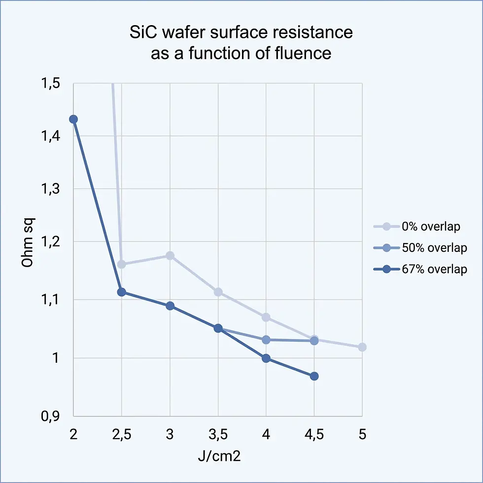
Silicon carbide (SiC) offers several advantages over silicon thanks to its wide band gap and improved properties at high temperatures, and is increasingly establishing itself as the base material for the manufacturing of modern high-performance semiconductor devices. The applied metal contacts initially form a Schottky contact, which limits the performance of the components. Localized heat treatment with UV lasers is used to produce targeted silicide transition layers that provide ohmic contacts and restore the performance of the components.
Our reliable line beam solutions for SiC annealing significantly increase throughput while maintaining the same footprint compared to conventional technologies.
Laser Drilling
Highly complex circuits between chips and chiplets require countless connections, which are routed on the circuit boards made out of ABF, FR4 or other materials in several layers. Mechanical drilling of the connections is limited by the available hole sizes and speeds. Laser drilling significantly increases the processing speed to several thousand holes per second and decreases the size to a diameters of down to 10 µm.
With our innovative optics for laser drilling, we are working on further reducing the hole diameter to the single µm range.
Laser Structuring and Marking
Precise structuring and marking of components is used in a variety of ways to functionalize or label components. The smallest structures in the µm range can only be produced using lasers.
Our optical solutions rely on UV to IR DPSS lasers and use the high-precision imaging of structuring masks to create high-precision holes, lines, and free-form structures in the micrometer range on dielectric materials and polymer-based substrates.
Thin Film Crystallization
Laser crystallization enables the modification of amorphous materials into a (poly)crystalline state in thin (semiconductor) layers. Compared to thermal processes, the laser has the advantage that the energy is deposited locally in a targeted manner and the pulse lengths in the ns range enable heating and cooling rates that are not possible with other technologies. Other properties of light, such as intensity distribution, pulse length and shape, and polarization, can be used to precisely tailor the crystallization process to the desired result.
This technology is used in particular in the semiconductor and OLED display industries and improves the electronic and optical properties of thin semiconductor layers.
Laser Lift Off
Laser lift-off (LLO, also known as laser debonding, UV laser release, or UV laser peeling ULP) enables the non-destructive and precise separation of thin functional layers such as (OLED) displays, flexible electronics, or wafers from the temporary carrier (mother glass or bonding wafer). This process step enables the production of modern OLED displays, but is also increasingly used in semiconductor manufacturing with ever thinner wafers. For debonding, the UV laser beam is focused through the UV-transparent carrier onto the interface with the functional layer. Due to the low penetration depth of the UV laser, the laser energy is deposited in a targeted manner and breaks the bond when the parameters are correct, so that the functional layer is detached without force or damage and without damaging the sensitive structures.
Our optical solutions rely on high-performance UV solid-state lasers (UV-DPSS), which have proven themselves in industrial use and offer high reliability, high productivity, and low operating costs.