


Solid State Laser Annealing for OLED Display
Systems > Solid State Laser Annealing
OLED Display Thin Film Transistor (TFT) Crystallization
Annealing, liquid and solid phase crystallization applications are of great importance for the preparation of silicon films for the production of large area electronics and semiconductor devices.
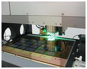
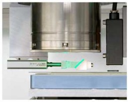
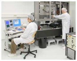
INNOVAVENT application lab exposure
OLED displays take advantage of the thin film transistor performance to switch the display pixel matrix. Driver electronics, memory and CPU circuits can be directly produced on the glass substrate. Thin silicon films are transferred into the liquid phase and controlled solidification results in homogenous crystallization providing high electron/hole mobility.
Thin film transistors (TFT) are built up in the p-Si film control the OLED current to generate the RGB picture.
The a-Si film electron mobility is enhanced by a factor of 500-1000 when generating the p-Si film from the a-Si.
UV laser light of 343nm wavelength is well absorbed in a 10nm a-Si and p-Si layer (>1.000.000cm-1).
UV-SLA (UV Solid State Laser Annealing) operates with 343nm. UV-SLA offers a break through in reduction of operating cost and maintenance time to substitute the “near complete melt” ELA (Excimer Laser Annealing) of a-Si films.
Prof James Im and coworkers from Columbia University published first results in the 90's (e.g. Robert S. Sposili, James S. Im, Sequential lateral solidification of thin silicon films on SiO2, Applied Physics Letters 69, p. 2864 (1996)) and several procedure patents were filed.
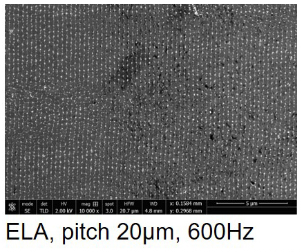
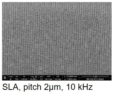
The 343nm UV-SLA process is very similar to the ELA process. The absorption in a-Si and p-Si is the same (as with 308nm). Multi shot absorption while scanning creates a uniform grain size distribution. The temporal pulse shape control and the scanning pitch of 2-3µm @ 10 kHz reduce the energy density to 250-300mJ/cm² compared to ~420mJ/cm² with excimer lasers. The FLATTOP profile in the scan axis of 40-50µm width allows to create the ELA typical grain pattern with the wavelength period.
UV-SLA provides the potential of enhanced uniform films through the small pitch of 2µm at 10kHz rep.-rate (20µm @ 600Hz for ELA) and this at higher throughput and reduced cost of ownership (40-50% of ELA).
A 750mm long line with a 50µm FLATTOP can be created by multiplexing 4 TruMicro 8340 (40mJ, 10 kHz), 15-20ns) with an energy density of >350mJ/cm². A line length of 1000mm is obtained with 6 TM 8340 lasers.
| Laser Optics for LCD and OLED Display | ||||